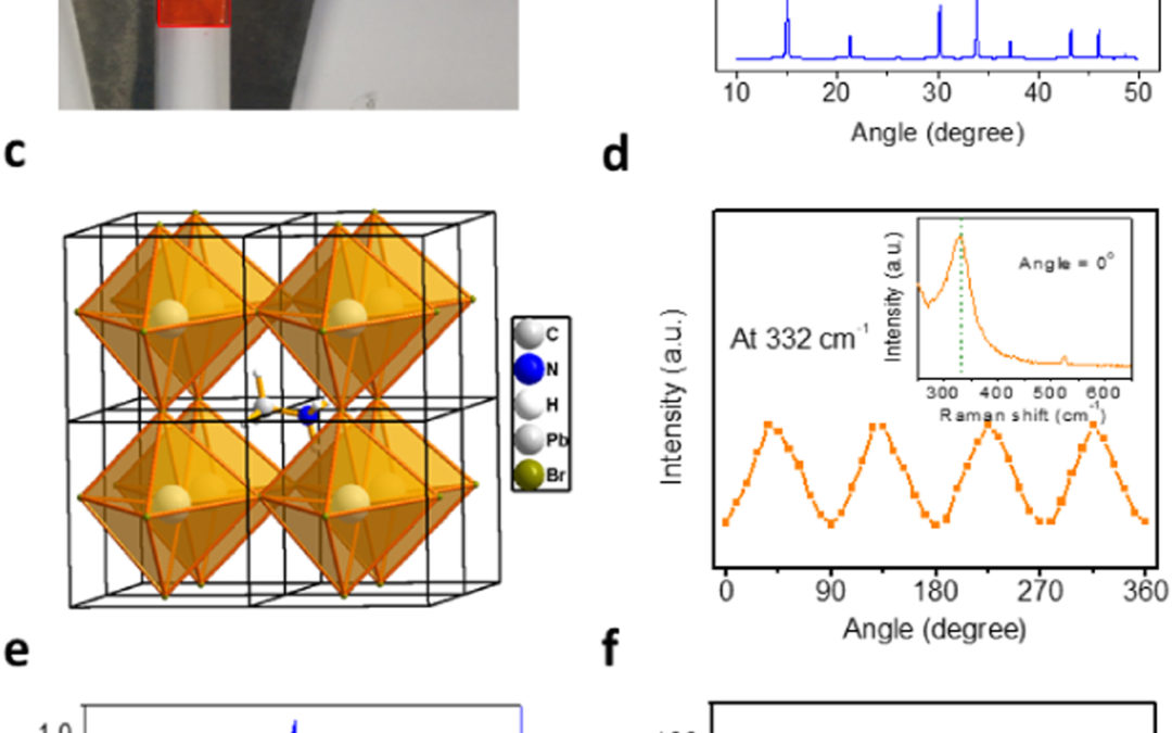
Organic-inorganic perovskites have arrived at the forefront of solar technology due to their impressive carrier lifetimes and superior optoelectronic properties. By having the cm-sized perovskite single crystal and employing device patterning techniques, and the transfer length method (TLM), we are able to get the insight into the metal contact and carrier transport behaviors, which is necessary for maximizing device performance and efficiency. In addition to the metal work function, we found that the image force and interface charge pinning effects also affect the metal contact, and the studied single crystal CH3NH3PbBr3 features Schottky barriers of 0.17 eV, 0.38 eV, and 0.47 eV for Au, Pt, and Ti electrodes, respectively. Furthermore, the surface charges lead to the thermally activated transport from 207 K to 300 K near the perovskite surface. In contrast, from 120 K to 207 K, the material exhibited three-dimensional (3D) variable range hopping (VRH) carrier transport behavior. Understanding these fundamental contact and transport properties of perovskite will enable future electronic and optoelectronic applications.
Read more at: Nano Energy, 53, pp. 817-827, 2018


Recent Comments