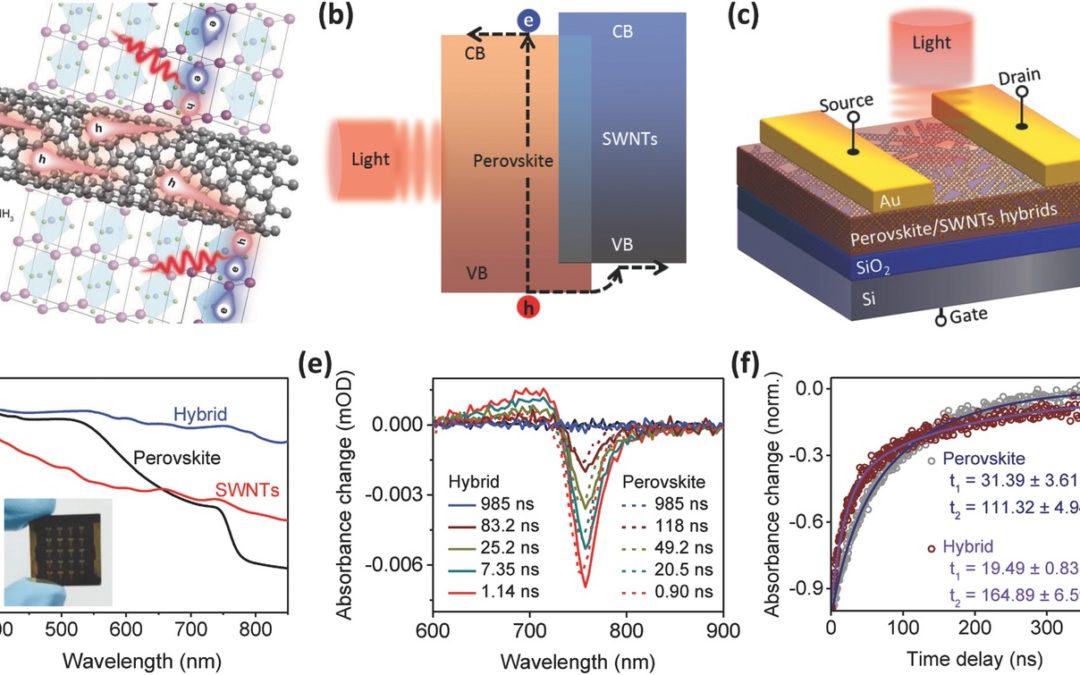
Organolead trihalide perovskites have drawn substantial interest for photovoltaic and optoelectronic applications due to their remarkable physical properties and low processing cost. However, perovskite thin films suffer from low carrier mobility as a result of their structural imperfections such as grain boundaries and pinholes, limiting their device performance and application potential. Here we demonstrate a simple and straightforward synthetic strategy based on coupling perovskite films with embedded single‐walled carbon nanotubes. We are able to significantly enhance the hole and electron mobilities of the perovskite film to record‐high values of 595.3 and 108.7 cm2 V−1s−1, respectively. Such a synergistic effect can be harnessed to construct ambipolar phototransistors with an ultrahigh detectivity of 3.7 × 10¹⁴ Jones and a responsivity of 1 × 10⁴ A W−1, on a par with the best devices available to date. The perovskite/carbon nanotube hybrids should provide a platform that is highly desirable for fields as diverse as optoelectronics, solar energy conversion, and molecular sensing.


Recent Comments