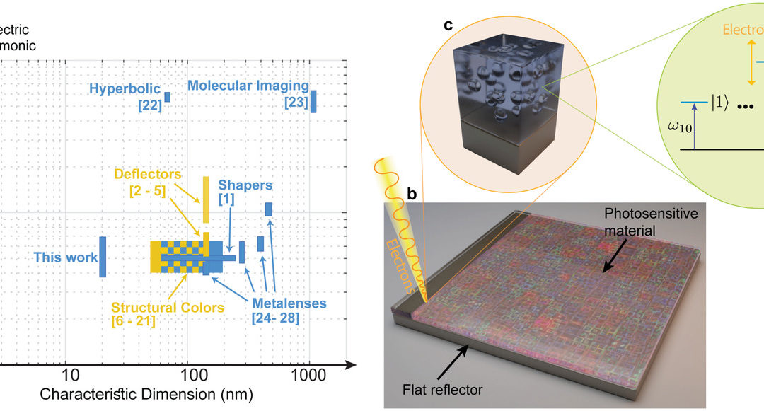
Controlling broadband light in nanoscale volumes is a desired goal in nanophotonics. Metastructures tackle this problem by subwavelength nanostructured patterns. The current technology reaches footprints of 50 nm with plasmonic nanostructures. Scaling down these values is challenging, especially in low loss dielectrics. Here, a new class of metasurfaces is introduced, “printed” point‐to‐point by free‐electron waves and created by altering the resonant atomic transition of inexpensive photosensitive materials. With this approach it is possible to directly write a desired distribution of refractive index and extinction coefficient with a resolution equal to the focusing accuracy of the electron beam, theoretically limited to the single nanometer. An application of this technology is illustrated in structural coloration. Currently, the best results are obtained with plasmonics at 127 000 dual polarization interferometry (DPI), with 50–200 nm structures and chromaticity ranging from blue to yellow. Free‐electron metasurfaces can generate the complete spectrum of colors of the cyan, yellow, magenta, and black system with resolutions up to 256 000 DPI, and nanostructures of 10 nm radius by using a single inexpensive layer of transparent material. This platform can enable a new generation of low cost transparent media supporting ultradense optical circuitry for broadband light control.
Read more in Advanced Optical Materials (early view).
Recent Comments